Published: February 12, 2026
By: Zhen Liu, Pure Copper Technical Expert at Cymber Metal
Hi everyone—Zhen Liu here, your pure copper specialist at Cymber Metal. When it comes to sputtering target copper—the “king” of high-purity copper for vacuum coating—it’s a different world from busbars or fittings. These targets need ultra-high purity (often 99.999% or higher) and perfect uniformity to deposit thin, defect-free films on semiconductors, displays, and solar cells. Even tiny impurities or grain variations can cause arcing or uneven coating, ruining expensive wafers.
In 2026, with semiconductor nodes shrinking and display tech advancing (OLED, mini-LED), demand for premium sputtering targets is stronger than ever. We’ve been supplying high-purity target copper at Cymber Metal for years, backing bonded to custom shapes. This guide shares what I’ve learned in the cleanroom and shop: purity levels, applications, challenges, and tips to get reliable, high-performance targets.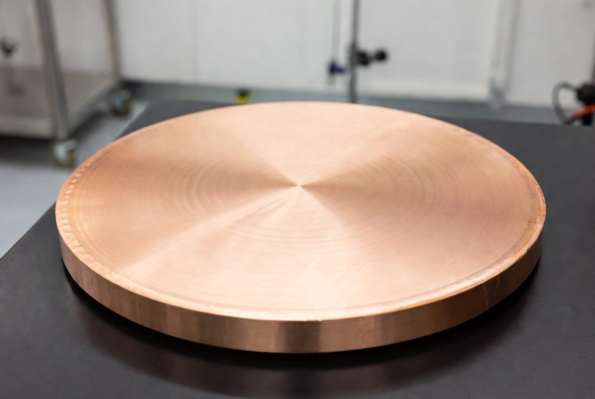
Sputtering Target Copper Purity Levels and Properties
Purity Classification Table
| Purity Level | Common Designation | Oxygen/Impurity Notes | Key Strengths | Suitable Applications | Relative Cost |
|---|---|---|---|---|---|
| 4N (99.99%) | Standard High-Purity | Low oxygen, controlled impurities | Good balance of cost and performance | General PVD coating, solar cells | Medium |
| 5N (99.999%) | Ultra-High Purity | Very low impurities | Excellent uniformity, low arcing | TFT-LCD, OLED displays | High |
| 6N (99.9999%) | Extreme Purity | Trace impurities <1 ppm | Maximum film quality, minimal defects | Advanced semiconductors, EUV lithography | Very High |
Quick Tip: 5N for most display and solar targets—6N when fabs demand zero defects in leading-edge chips.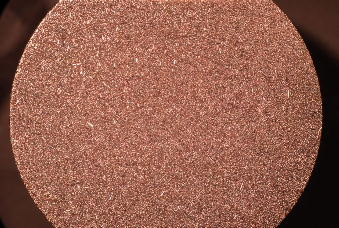
Key Applications of Sputtering Target Copper
Sputtering targets deposit copper films in vacuum—critical for interconnects and barriers.
Semiconductor Interconnects and Barriers
Copper layers in chips for wiring—low resistivity and high electromigration resistance.
Display Panel Coating (TFT-LCD, OLED)
Gate, source/drain lines in panels—uniform films for bright, reliable screens.
Solar Cell Metallization
Back contact and grid lines—efficient current collection in thin-film PV.
Optical and Decorative Coatings
Reflective layers in mirrors or architectural glass.
Touchscreen and Flexible Electronics
Conductive traces in sensors and foldable devices.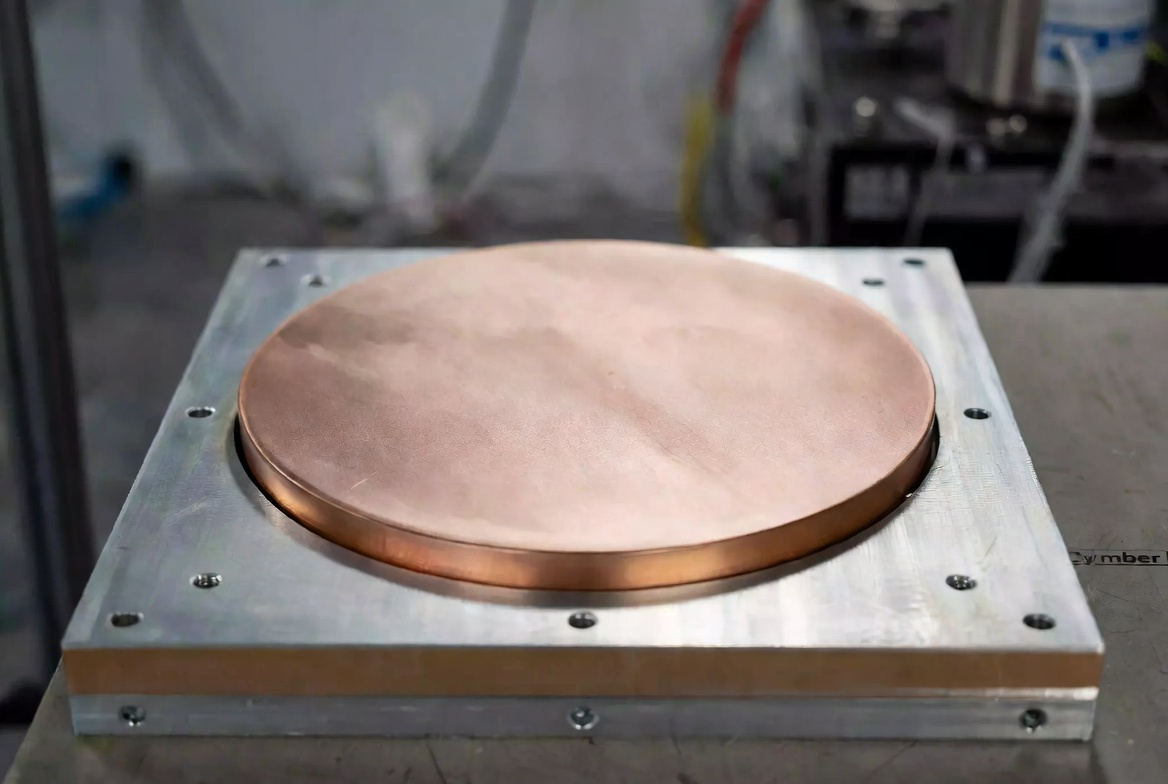
Challenges in Manufacturing Sputtering Target Copper
Purity and Uniformity Issues
- Impurities causing arcing → Defects in deposited films.
- Grain size variation → Uneven sputtering rates.
- Oxygen inclusion → Voids and poor adhesion.
Practical Shop Solutions
Engineering Experience: In our sputtering target projects at Cymber Metal for a major display maker, early 5N blanks had slight grain variation causing non-uniform erosion. We refined our vacuum melting and hot isostatic pressing—achieving <5% variation across the target and zero arcing reports in production runs.
Pro Tip: Always inspect grain structure post-forging—it’s the key to consistent sputter rates.
Design and Processing Tips for Targets
- Shapes: Rectangular, circular, rotary—match chamber design.
- Bonding: Indium or elastomer to backing plate.
- Surface Finish: Ra <0.4 µm for clean start.
Tooling & Parameter Recommendations
- Melting: Vacuum induction for purity.
- Forming: HIP or forging for density.
- Machining: Light cuts on bonded targets.
-
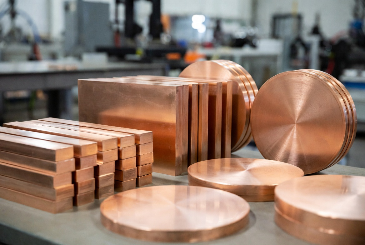
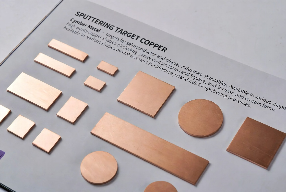
Common Deliverable Sputtering Target Copper Forms
- Rectangular planar targets
- Circular and rotary targets
- Custom shaped targets
- Bonded target assemblies
- Backing plate integrated targets
Real-World Applications
- Semiconductor Cu interconnects
- Display electrode layers
- Solar cell contacts
- Optical reflectors
- Touch panel conductors
Cost & Sustainability Factors in 2026
High-purity targets premium-priced, but recycling of used targets and backing plates reducing waste.
Final Thoughts
Sputtering target copper solves the toughest purity and uniformity challenges in thin-film deposition—enabling the next generation of chips, displays, and solar cells.
At Cymber Metal, we specialize in high-purity sputtering target copper:
Visit our CYMBER Copper Bar & Busbar Core Warehouse to see our full stock and capabilities.
If you’re sourcing sputtering target copper—whether square, busbar-style, custom shapes, or bonded assemblies—Cymber Metal offers ultra-high purity material, precise manufacturing, and flexible volumes.
Ready to discuss your coating project? Download our target copper catalog or contact our team.
Post time: Feb-12-2026